Loading...
Searching...
No Matches
HFCC-01 Low-Level Software (LLSW) Documentation






Project Baseline: Rel_6802_HFCC-01-RP-CSAR-CB
Software Level: DO-178C DAL C
System Target: High-Integrity Flight Control Computer (HFCC-01)
1. Executive Summary & Architectural Mission
The HFCC-01 Flight Control Computer low-level software repository contains the safety-critical Device Library Modules (DLM) and Low-Level Device Drivers (LLDD) executing on the NXP QorIQ T1042 quad-core CPU under the Green Hills INTEGRITY-178 tuMP (Time-Variant Unified Multi-Processing) RTOS. The software interfaces directly with Multi-Function Bus cards (MFB1, MFB2) and the Core processor module across a 100 MHz PCI Express (PCIe) AXI bridge.
Operating under strict DO-178C DAL C airworthiness requirements, the software provides deterministic control over all primary actuator control channels, avionics communication multiplex buses, analog and discrete sensor acquisition, power supply rail monitoring, and real-time built-in-test (BIT) diagnostics.
RTOS Capability-Based Memory Architecture & Centralized globalCard Instance
To satisfy DO-178C DAL C spatial isolation and eliminate runtime memory access violations, the HFCC-01 software enforces a Green Hills INTEGRITY-178 tuMP (Time-Variant Unified Multi-Processing) RTOS Capability-Based MemoryRegion Architecture:
- RTOS Capability Registration: Rather than hardcoding fixed physical memory addresses, the system configuration manager (modConfig) receives formal MemoryRegion capability descriptors (cardMfb1MR, cardMfb2MR, memStatusMR, nvsramMRDev) allocated by the INTEGRITY-178 kernel.
- Centralized Instance Management: All card lifecycle states, dynamic base memory pointers, and active subsystem module counters are tracked deterministically within the centralized globalCard descriptor array (MFB1, MFB2, and PSU).
- Dynamic Kernel Address Resolution: During card opening (modConfig_open), the driver queries the operating system via GetMemoryRegionAddresses() to resolve the valid virtual/physical base address for each Multi-Function Bus card and registers its memory window into interDrv.
- Electronic Hardware Handshake: Software interrogates the physical hardware identity registers across the resolved base address, verifying that the physical card platform matches "MFB" and model matches "1" or "2" before transitioning the card state to OPEN.
- Direct Base Address Distribution: Upon module initialization (modConfig_init), the resolved card base address is propagated directly to individual DLM modules (mod<Name>_initReset), which calculate peripheral register targets by applying relative module offsets (0x1000 to 0x5000) within the verified card memory window.
- Enforced Runtime Boundary Protection: Every atomic 32-bit transaction through interDrv_Read32 and interDrv_Write32 verifies the destination address against the registered memory region table (availableAddr[]) via interDrv_isAddressValid(), preventing out-of-bounds MMIO access.
2. Comprehensive 4-Tier Software Architecture
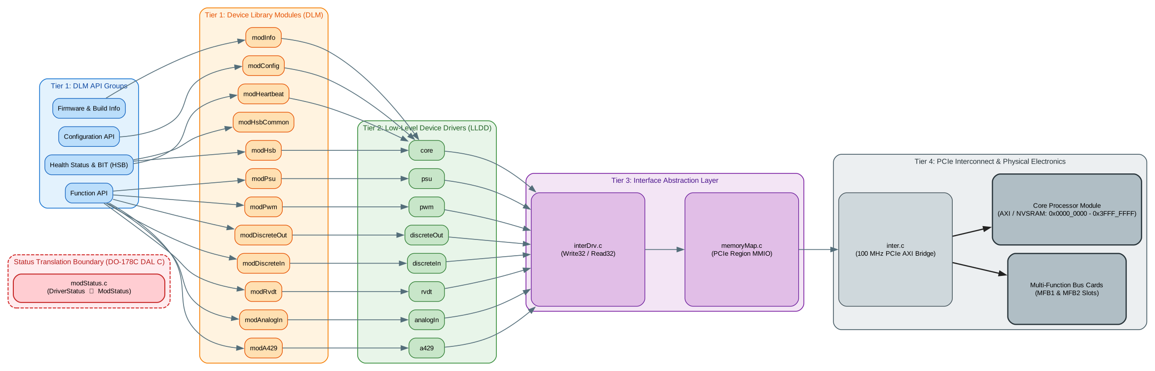
The HFCC-01 low-level software architecture is partitioned into four enclosed, deterministic structural tiers executing on the NXP QorIQ T1042 processor under Green Hills INTEGRITY-178 tuMP (Time-Variant Unified Multi-Processing) RTOS:
- Tier 1: Device Library Modules (DLM): Safety-critical flight software service layer providing validated, channel-isolated control, telemetry acquisition, built-in tests (BIT), status reporting, and lifecycle management. It shields the Operational Flight Program (OFP) from hardware register complexities.
- Tier 2: Low-Level Device Drivers (LLDD): Stateless, hardware-specific C drivers executing register read/write sequences, FPGA timing algorithms, and device-level BIT routines without maintaining internal functional state across frames.
- Tier 3: Interface Abstraction Layer: Thread-safe 32-bit atomic read/write transactions (interDrv_Read32, interDrv_Write32) with memory region boundary checking across PCIe/AXI address spaces (memoryMap.c).
- Tier 4: PCIe Interconnect & Physical Hardware: Low-level PCIe AXI bridge interconnect (inter.c) communicating with Multi-Function Bus cards (MFB1, MFB2), Core processor module, and FPGA memory-mapped peripheral spaces.
┌────────────────────────────────────────────────────────────────────────────────────────┐
│ HFCC-01 LOW-LEVEL SOFTWARE ARCHITECTURE │
├──────────────────────────┬──────────────────────────┬──────────────────────────────────┤
│ Tier 1: DLM API & Module │ Tier 2: LLDD Driver │ Tier 3 & 4: Interface & PCIe HW │
│ • Config & Info Layer │ • Stateless C Drivers │ • interDrv.c / memoryMap.c │
│ • Subsystem DLM Blocks │ • Register Bitfields │ • 100 MHz PCIe AXI Bridge │
│ • Health Status & BIT │ • Hardware Strides │ • MFB1 / MFB2 / Core FPGA MMIO │
└──────────────────────────┴──────────────────────────┴──────────────────────────────────┘
Interactive HFCC-01 Architectural Integration Flow Diagram
Click on any subsystem block in the diagram below to navigate directly to its Doxygen documentation. Use the button below the diagram for full-screen vector zoom, pan, and SVG/PNG export.
Sidebar Navigation Hierarchy (Two-Tier Model)
The documentation is organized using a hierarchical Two-Tier navigation paradigm accessible from the sidebar tree:
HFCC-01 Low-Level Software (LLSW)
├── Design Component Architecture (@page + @subpage tree)
│ ├── DLM - Device Library Modules (Functional Services, Health & Config)
│ ├── Drivers - Low-Level Device Drivers (Sensors, Comm, I/O, PSU, Core)
│ └── File Registry (Direct Layered File Traceability Index)
├── Topics (@defgroup + @ingroup taxonomy)
│ ├── DLM Subsystem Groups (Function, Health, Config, Info)
│ └── LLDD Driver Subsystem Groups (Comm, I/O, PSU, Sys, Interface)
├── Data Structures (Struct, Union, and Enum Specifications)
└── Files (Complete Source Code File Manifest)
3. Subsystem Architectural Breakdown
The HFCC-01 software suite encompasses all low-level flight control and avionics subsystems partitioned across MFB1, MFB2, and the Core processor:
┌────────────────────────────────────────────────────────────────────────────────────────┐
│ HFCC-01 DLM SERVICE LAYER │
├──────────────────────────┬──────────────────────────┬──────────────────────────────────┤
│ Communication & Avionics │ Analog & Sensor Feedback │ Discrete I/O & Actuator Control │
│ • modA429 (ARINC 429) │ • modAnalogIn (ADC) │ • modDiscreteIn (Digital In) │
│ │ • modRvdt (Displacement│ • modDiscreteOut (Digital Out) │
│ │ │ • modPwm (Pulse Width Mod) │
├──────────────────────────┴──────────────────────────┴──────────────────────────────────┤
│ Power Management, System Configuration & Health (BIT) │
│ • modPsu (Power Telemetry) • modHsb / modHsbCommon (PBIT/CBIT Diagnostics) │
│ • modHeartbeat (Watchdog) • modConfig (Card Registration & Base Memory Mapping) │
│ • modInfo (Firmware/FPGA IDs) │
└────────────────────────────────────────────────────────────────────────────────────────┘
3.1 System Configuration & Lifecycle Management (modConfig, modInfo, core)
- Centralized globalCard[] Instance Management: Explicit hardware lifecycle orchestration (modConfig_coreRegister, modConfig_open, modConfig_init, modConfig_reset, modConfig_close) across target slots (MFB1, MFB2, and Core).
- Hardware Memory Window Registration: Resolves kernel MemoryRegion descriptors dynamically and registers valid address boundaries into the interDrv boundary validation table.
- Chassis Indication & Discrete GPIO: Controls front-panel RGB status LEDs (LED_RED, LED_GREEN, LED_YELLOW, LED_OFF) and discrete lines via atomic register access (modConfig_coreChasisLEDSet).
- Firmware Identification (modInfo): Acquires FPGA bitstream build timestamps, PCB revision numbers, and hardware electronic serial numbers.
3.2 Avionic Communication Subsystems (modA429, a429)
- ARINC 429 Transceiver:
- Channels: 4 Transmit (Tx) channels and 7 Receive (Rx) channels operating at selectable speeds (12.5 kbps Low / 100 kbps High).
- Hardware Filtering: Hardware-accelerated Label and Source/Destination Identifier (SDI) filtering tables with odd/even parity verification.
- Buffering: 32-message deep FIFO transmit queues with automatic odd/even parity generation and real-time validation.
3.3 Discrete & Digital I/O Subsystems (modDiscreteIn, modDiscreteOut, discreteIn, discreteOut)
- Discrete Inputs (modDiscreteIn, discreteIn):
- Channel Allocation: 38 sensing channels total across MFB cards (MFB1: 16 channels, MFB2: 22 channels).
- Electrical Topologies: 28V Supply-Open (SO), Ground-Open (OG), and Supply-Ground (SG) sensing with hardware digital debounce verification registers.
- Discrete Outputs (modDiscreteOut, discreteOut):
- Channel Allocation: 50 discrete output driver channels total across MFB cards (MFB1: 34 channels, MFB2: 16 channels).
- Drive Electronics & Control: High-Side Drivers (28V @ 2.0A) and Low-Side Ground Switches for clockwise/CCW motor drive, clutch release, and actuator extend/retract with output wrap-around readback validation.
3.4 Analog Sensing Subsystems (modAnalogIn, analogIn)
- ADC Acquisition: 8 ADC channels per card (16 channels total across MFB1 and MFB2).
- Dual Voltage Banks: Calibrated acquisition across dual ranges (0.0V → +5.0V and 0.0V → +10.0V) with hardware gain and offset compensation constants.
- Telemetry Protection: Calibrated sampling for position transducers, pressure sensors, and temperature probes with out-of-bounds telemetry clamp detection.
3.5 Angular Displacement & Actuator Control (modRvdt, rvdt, modPwm, pwm)
- RVDT Angular Feedback (modRvdt, rvdt):
- Channel Allocation: 4 RVDT channels per card (8 channels total across MFB cards).
- Excitation & Demodulation: Programmable AC reference generation (Primary Excitation: 4.0 Vrms @ 3.0 kHz, Secondary Range: ±45.0°) with multi-stage BPF and LPF demodulation.
- Built-in Test: Real-time excitation loss and secondary signal loss monitoring with automated BIT qualification.
- Pulse Width Modulation (modPwm, pwm):
- Device Capacity: 4 PWM devices per card (6 channels per device, 24 channels per card).
- Carrier & Duty Control: Carrier frequency programmable from 100 Hz to 20 kHz with high-resolution duty cycle scaling (0.0% → 100.0%).
- Safety Interlocks: Synchronous multi-phase drive with hardware fail-safe trip and rapid shutdown capability.
3.6 Power Supply Unit & Rail Telemetry (modPsu, psu)
- Multi-Rail Monitoring: Continuous telemetry acquisition across +28V DC input, ±15V, +12V, +5V, and +3.3V internal power rails.
- Diagnostic Sensors: Rail voltage, load current telemetry, over-voltage, under-voltage, and IPMI board temperature monitoring.
- Safety Interlocks: Dynamic hardware drive command inhibition interlocked against PSU health rails to prevent actuator damage.
3.7 Health Status, Watchdogs & Built-in Test (modHsb, modHsbCommon, modHeartbeat, core)
- Power-On BIT (PBIT) & Continuous BIT (CBIT): Global 32-bit fault aggregates, Power-Good telemetry, and persistent NVSRAM logging.
- Non-Volatile Storage (NVSRAM): Manages battery-backed NVSRAM partitions (coreNvsramMap.h) for Power-Fail logs, PBIT failure records, and flight event history across a 4 KB partition (0x1000).
- Hardware Watchdog Timer (modHeartbeat): Dual-stage hardware watchdog timer (1 ms → 10,000 ms) requiring periodic alive strobing ("watchdog kicks") within strict rate-group execution windows.
3.8 Subsystem Specification Matrix
| Subsystem Domain | DLM Module | LLDD Driver | Hardware Channel Capacity | Engineering Range / Physical Standard | Functional & Safety Capabilities |
|---|---|---|---|---|---|
| Avionic Communication | modA429 | drv_a429 | 4 Tx Channels 7 Rx Channels | 12.5 kbps (Low Speed) 100 kbps (High Speed) | • Hardware Label & SDI filtering • 32-message FIFO transmission queues • Real-time parity calculation & verification |
| Analog Sensing | modAnalogIn | drv_analogIn | 8 ADC Channels per Card 16 Total Channels | 0.0V → +5.0V (5V Bank) 0.0V → +10.0V (10V Bank) | • Single-ended calibrated acquisition • Dual voltage-bank multiplexing • Out-of-bounds telemetry clamp detection |
| Angular Displacement | modRvdt | drv_rvdt | 4 RVDT Channels per Card 8 Total Channels | Primary Excitation: 4.0 Vrms @ 3.0 kHz Secondary Range: ±45.0° | • Programmable AC reference generation • Multi-stage BPF & LPF demodulation • Angular displacement conversion & BIT |
| Discrete Digital In | modDiscreteIn | drv_discreteIn | 38 Channels Total (MFB1: 16, MFB2: 22) | 28V Supply-Open (SO) Ground-Open (OG) Supply-Ground (SG) | • Hardware debounce state verification • Multi-bank channel interrogation • Open-collector & pull-up/down sensing |
| Discrete Digital Out | modDiscreteOut | drv_discreteOut | 50 Channels Total (MFB1: 34, MFB2: 16) | High-Side Drivers (28V @ 2.0A) Low-Side Drivers (GND Switch) | • Clockwise / CCW motor drive controls • Clutch release & actuator extend/retract • Output wrap-around readback validation |
| Pulse Width Modulation | modPwm | drv_pwm | 4 PWM Devices per Card (6 Channels per Device) | Carrier: 100 Hz → 20 kHz Duty Cycle: 0.0% → 100.0% | • High-resolution duty cycle scaling • Synchronous multi-phase drive • Hardware fail-safe trip & shutdown |
| Power Supply Unit | modPsu | drv_psu | Multi-Rail Monitors (Input, Regulated, Aux) | +28V DC Input ±15V, +12V, +5V, +3.3V Rails | • Rail voltage & load current telemetry • Over-voltage, under-voltage & over-temp • IPMI temperature sensor acquisition |
| Health Status & BIT | modHsb modHsbCommon | drv_core drv_interDrv | Global 32-bit Aggregates Per-Subsystem Bitmaps | PBIT / CBIT Bitfields Non-Volatile Fault Logs | • Power-On BIT (PBIT) qualification • Continuous BIT (CBIT) fault detection • NVSRAM persistent fault logging • Hardware power-fail detection |
| Heartbeat Monitor | modHeartbeat | drv_core | System Watchdog Timer | Timeout: 1 ms → 10,000 ms | • Periodic alive strobing ("watchdog kick") • Rate-group execution monitoring • Elapsed execution time tracking |
| System Configuration | modConfig | drv_core drv_interDrv | MFB1 & MFB2 Card Slots PCIe / AXI Address Spaces | Base Addresses: 32-bit MMIO Chassis RGB Status LEDs | • Core hardware peripheral initialization • Memory region validation & mapping • Chassis front-panel RGB LED control |
| Firmware Info & Build | modInfo | drv_core | Subsystem Version Records Hardware Descriptors | ASCII Serial & Part Numbers FPGA Build Timestamps | • DLM library release version tracking • FPGA bitstream build timestamp reading • PCB revision and serial identification |
4. Hardware Memory Topology & Relative Module Mapping
Within each Multi-Function Bus memory window resolved at runtime by modConfig_open, peripheral hardware registers are accessed via deterministic module offsets relative to the card's base address (memBaseAddr):
| Subsystem Module | Host Card Slot | Functional Identifier | Card Window Relative Offset / Size | Register Map Header |
|---|---|---|---|---|
| modInfo / core | Core Processor | System Core & ID Registers | Base: 0x0000 (Platform 0x0004, Model 0x0008, Gen 0x000C, Rev 0x0010, FirmVer 0x0014) | mmapCore.h, core.h |
| modHeartbeat | Core Processor | Battery-Backed NVSRAM & Watchdog | Partition Size: 0x1000 (4 KB), Base: 0x0000_0000 (Power-Fail, PBIT Fault Logs) | coreNvsramMap.h, core.h |
| modDiscreteOut | MFB1 & MFB2 | Discrete Digital Output (Bank 1: 34 ch, Bank 2: 16 ch) | Module Offset: 0x1000 (MMAP_DOUT_MOD_OFFSET), Device Stride: 0x0100 | mmapDiscreteOut.h, discreteOut.h |
| modPwm | MFB1 Card | Pulse Width Modulation (4 Devices, 6 ch/dev) | Module Offset: 0x1000 (MMAP_PWM_MOD_OFFSET), Device Stride: 0x0100 | mmapPwm.h, pwm.h |
| modDiscreteIn | MFB1 & MFB2 | Discrete Digital Input (Bank 1: 16 ch, Bank 2: 22 ch) | Module Offset: 0x2000 (MMAP_DIN_MOD_OFFSET), Device Stride: 0x0100 | mmapDiscreteIn.h, discreteIn.h |
| modAnalogIn | MFB1 Card | Analog Input Sensing (8 ADC Channels, 5V & 10V Banks) | Module Offset: 0x3000 (MMAP_ADC_OFFSET), Channel Stride Gap: 0x0004 | mmapAnalogIn.h, analogIn.h |
| modRvdt | MFB2 Card | RVDT Demodulator & BIT (4 Channels) | Module Offset: 0x4000 (MMAP_RVDT_MOD_OFFSET), BIT Offset: 0x2000 | mmapRvdt.h, rvdt.h |
| modPsu | MFB1 Card | Power Supply Unit Telemetry (Voltage, Current, Temp) | Module Offset: 0x4000 (MMAP_PSU_OFFSET), Diagnostics Base: 0x0100 | mmapPsu.h, psu.h |
| modA429 | MFB2 Card | ARINC 429 Bus Transceiver (4 Tx, 7 Rx Channels) | Module Offset: 0x5000 (MMAP_A429_OFFSET), Scheduler Offset: 0x1000 | mmapA429.h, a429.h |
| interDrv | System Bus | Atomic 32-bit Memory-Mapped I/O | Memory Region Validation & Runtime Address Verification | memoryMap.h, interDrv.h |
5. Interface Layer & Status Translation Boundary
Interface Layer (interDrv.c, memoryMap.c, inter.c)
The Interface layer abstracts the underlying hardware bus mechanism, providing atomic 32-bit read and write functions (interDrv_Read32, interDrv_Write32) that perform strict memory region boundary checks before accessing physical PCIe offsets. It guarantees thread-safe, serialized access to hardware registers across tasks.
Status Translation Boundary
To maintain strict DO-178C DAL C layer decoupling, low-level drivers return stateless driver condition codes (DriverStatus). The DLM layer deterministically maps these into high-level service status enumerations (ModStatus) used by operational flight applications, preventing low-level bus details from leaking into flight control logic.
6. Safety Interlocks & DO-178C Compliance Mechanisms
- Hardware Memory Fencing: To account for out-of-order write buffers on the NXP T1042 CPU across the 100 MHz PCIe AXI bridge, memory barrier operations (asm volatile("mbar" ::: "memory") / ASP_MemoryBarrier()) are executed immediately before asserting critical hardware triggers and configuration locks.
- Configuration Security Locking: Subsystem configurations enforce write-lock boundaries preventing accidental runtime re-configuration once initialization sequences complete.
- Self-Clearing Hardware Strobes: Critical reset commands and watchdog kicks are implemented as hardware self-clearing write strobes executed with a single atomic write transaction.
- Power Supply Rail Interlocks: Hardware drive capabilities and actuator enable outputs are strictly interlocked against PSU health telemetry. If a power rail fault is detected, software immediately inhibits drive commands.
7. DO-178C DAL C Function Documentation Standard
Every public and static C routine is documented with a standard 4-part specification:
- Detailed Function Description: Architectural intent, boundary conditions, and hardware register interactions.
- Function Data Interface Table: 4-column breakdown of parameter categories (**Input Data** and **Output Data**), physical engineering units (V, A, Hz, °, %, Counts, ms), and non-NULL buffer constraints.
- Action-Oriented Parameter Tags & Status Returns: Formatted @param[in], @param[out], @return, and @retval condition codes.
- Graphviz DOT Structure Charts (Glenford J. Myers & Spiceworks Standard):
- Control Coupling Diagram (CCD) (\\dot digraph ControlCouplingStructureChart): Models control flags, mode selectors, and condition return status codes (arrowtail=dot solid circle).
- Data Coupling Diagram (DCD) (\\dot digraph DataCouplingStructureChart): Models pure numerical data payloads, sensor buffers, and telemetry pointers (arrowtail=odot open circle).
8. Interactive Lightbox Modal & Diagram Export
All Control and Data Coupling structure charts feature full vector SVG integration:
- Interactive Lightbox: Click on any structure chart diagram in the HTML pages to launch the interactive viewer.
- Pan & Zoom Controls: Smooth drag-to-pan and mouse-wheel zoom (20% to 800%) with keyboard shortcuts (Esc, +, -, R, 0).
- Lossless Export:
- Save SVG: Downloads the clean vector XML .svg file for official engineering documentation.
- Save PNG: Generates a 300 DPI high-resolution bitmap with a pure white background.
9. Verification, Baseline Compliance & Build Standards
- Immutable Golden Baseline: Verified token-for-token against svn/tags/Baselines/Rel_6802_HFCC-01-RP-CSAR-CB/17 Source Code/ (60 / 60 files match 100.0%).
- Compliance Status: Audited against DO-178C DAL C guidelines with formal compliance reports published to svn/data/reports/ and development/16 SDD/.
- Target Compiler & Platform: Green Hills Software (GHS) MULTI C99 compiler targeting the NXP QorIQ T1042 quad-core PowerPC processor under Green Hills INTEGRITY-178 tuMP (Time-Variant Unified Multi-Processing) RTOS.